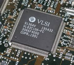
What is VLSI ?
VLSI ( Very Large Scale Integration ) Circuits is the Collection of More Than
One Million Small Chips Integrated on Single Large Chip. Initially These Chips
are Designed in Small Scale and After Designing and Testing Each modules
They are Fabricated in Single Large Chip. This Single Large Chip is
Known as VLSI Circuits.
Ex. Microprocessor
VLSI Design Cycle
To Design a Large VLSI Chip, It Follows a Some Steps Which are
given Under The Following Points.
1. System Specification
2. Architectural design
3. Functional design
4. Logic design
5. Circuit design
6. Physical Design
7. Fabrication
8. Packing and Testing
1. System Specification
In The First Step of VLSI Life Cycle, We Design High Level Functional
Description of The Circuits With Some Constraints Like Size, Speed,
and Power.
2. Architectural Design
In Architectural Design, We Design Micro-architectural Specification of The
Design With Architecture Style, Number of ALUs, Floating Point Units,
Number and Structure of Pipelines, and Size of Caches.
3. Functional Design
In Functional Design of VLSI Life Cycle We Concentrate on Functionality
of Each Individual Unit and Their Interconnection. The Area, Power,
and Time of Each Unit is Identified.
4. Logic Design
It Consists of Boolean Expressions and Timing Information of the Each
Individual Units.
5. Circuit Design
After Design of the Boolean Expressions and Timing Information of Each
Individual Unit, Circuit Description in Logic Gates is Generated.
6. Physical Design
Circuit Representation of the Individual Units is Converted into a Geometric
Representation. This Geometric Representation is Known as Layout of
The Circuits.
7. Fabrication
Output of the Physical Design Phase Will Works as a Input of the Fabrication
Phase. so after a layout is generated the design is ready for actual fabrication
or manufacturing.
8. Packing , Testing and Debugging
This is the Last Phase of the VLSI Design. After The fabrication or
Manufacturing of the Chip, Chips are ready for Packaging, Testing,
and debugging.
VLSI PHYSICAL DESIGN
For the Detailed Study of the VLSI Physical Design, you refer the
Following Presentation.
Thank You To All My Reader
Deepak Gupta
www.i-world-tech.blogspot.in
Related Post
1. First Program in JSP
2. Mini Project in C : Book Shop Inventory System
3. Interesting C++ Program
4. How To Install JDK on Windows
5. How we Install Apache Tomcat Server
6. Content Management System ( CMS )
7. JavaScript Form Validation
8. In Visual Basic : How we Convert our statement in Computer Voice
9. JavaScript Math Object
10. Batch Programming :How To make a Simple Calculator in Batch programming

Comments
Post a Comment